So, I finally got hold of one, se the TTY-section for mor information
Category Archives: Uncategorized
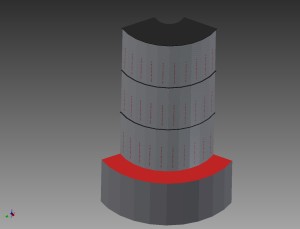
Played around with Inventor, a little bit
The ALU-schematics is not correct
I found out during simulation today, that the schematic posted earlier is incorrect.
The /AND and AND signals should be inverted, so here is a new schematic.
And the ALU Main ALU
The Design, Part 2: The ALU.
I have nearly completed the initial design of the ALU.
There are still some bits missing, and I havent simulated the whole ALU yet, only partly att block-level
It will support the following primitive functions:
- AND
- OR
- NOR
- XOR
- ADD
- SUB
- SLT
Here is a screenshot of the ALU
And the more readable pdf-file Main ALU
There is also a register section, 3 registers (at the moment) one bit per slice.
The pdf: Registers
There is three register A, B and Result.
the registers consist of one D Flip-Flop, per gate together with demultiplexers for selecting the function
The following operations is supported, it probably will be changed in the future:
- CPYMA (copy from Data-bus to A)
- CPYMB
- CPYRM ( Copy Result to Data-bus)
- CPYRA (Copy Result to A)
- CPYRB
When you look at the schematics, it might be a Little bit strange, but using ECL has an advantage compared to other families, The complementary output is easily accessible, which means that I can use that to reduce the number of gates needed.
For example, if I need an 2-input AND-Gate, you will use two inverters on the input of a NOR-Gate, thus, using the inverted output off the previous gate, instead of the normal output, I can omitt the inverters, saving two gates (Three transistors per gate).
This is basically what will go on each ALU-Slice Circuit board, together with the Biasing Circuit (I am also playing with the Idea of having a common Bias Circuit for the whole computer).
Apart from the above, there will also be a separate PCB for Look-Ahead Carry, as well as status register and Zero detecting Circuit.


![Mixed-Mode Simulator ( Circuit _ 1-BIT_ALU - Page _ MAINPAGE ) [Project _ ECL] Page _ 1](http://www.microdiscray.com/wp-content/uploads/2014/07/Mixed-Mode-Simulator-Circuit-_-1-BIT_ALU-Page-_-MAINPAGE-Project-_-ECL-Page-_-1-300x212.jpg)
![Schematic Editor ( Circuit _ 1-BIT_ALU - Page _ MAINPAGE ) [Project _ ECL] Page _ 1](http://microdiscray.com/wp-content/uploads/2014/07/Schematic-Editor-Circuit-_-1-BIT_ALU-Page-_-MAINPAGE-Project-_-ECL-Page-_-1-300x212.jpg)
![Schematic Editor ( Circuit _ 1-BIT_ALU - Page _ REG ) [Project _ ECL] Page _ 1](http://microdiscray.com/wp-content/uploads/2014/07/Schematic-Editor-Circuit-_-1-BIT_ALU-Page-_-REG-Project-_-ECL-Page-_-1-300x212.jpg)